Carol.inntraltd@gmail.com
EN
Ka
Products
Manufacturer
Place Order
Information
local
About Us
Corporate culture
Company introduction
Contact Us
Contact us
取消
Home
Products
Manufacturer
Place Order
Information
About Us
Contact Us
EN
Ka
New Arrivel Today(1)
Resistors(1464842)
Capacitors(1233524)
Inductors, Coils, Chokes(160301)
Potentiometers, Variable Resistors(31938)
Transformers(15404)
Crystals, Oscillators, Resonators(755151)
Discrete Semiconductor Products(252065)
Sensors, Transducers(174312)
Integrated Circuits (ICs)(656537)
RF and Wireless(109622)
Resistor Networks, Arrays(35407)
Accessories(263)
Chip Resistor - Surface Mount(896336)
Through Hole Resistors(507425)
Chassis Mount Resistors(24591)
Specialized Resistors(820)
Precision Trimmed Resistors(0)
Capacitor Networks, Arrays(2073)
Aluminum Electrolytic Capacitors(119232)
Tantalum Capacitors(106098)
Ceramic Capacitors(802073)
Previous
Next
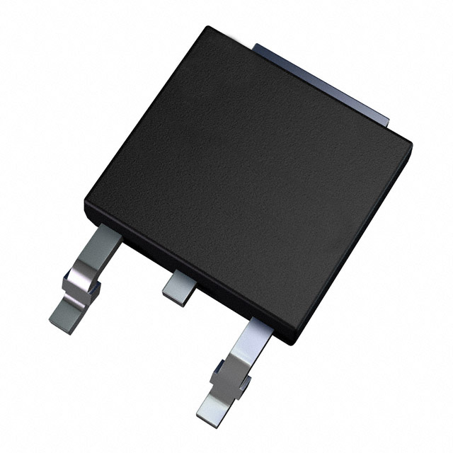
1SMB5928BT3G
K2200G
Wickmann / Littelfuse
W682310SG TR
Nuvoton Technology Corporation
ADCMP565BPZ
Linear Technology (Analog Devices, Inc.)
PDB-C171SM
Luna Optoelectronics (Advanced Photonix)
ECS-VXO-73-44.736-TR
ECS Inc. International
SK012DTP
Wickmann / Littelfuse
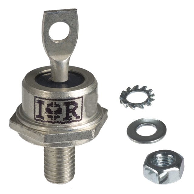
VS-40HFL10S02
Vishay General Semiconductor – Diodes Division
1SMB5928BT3G
ON SEMICONDUCTOR 1SMB5928BT3G Single diode Zener, general purpose, 13 V, 3 W, DO-214AA, 5 %, 2-pin, 150 °C
Details
K2200G
SIDAC 205-230V 1A DO15
Wickmann / Littelfuse
Details
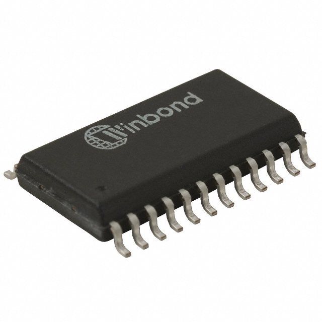
W682310SG TR
IC VOICEBAND CODEC 3V 2CH 24SOP
Nuvoton Technology Corporation
Details
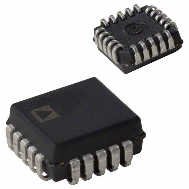
ADCMP565BPZ
IC COMPARATOR 2 W/LATCH 20PLCC
Linear Technology (Analog Devices, Inc.)
Details
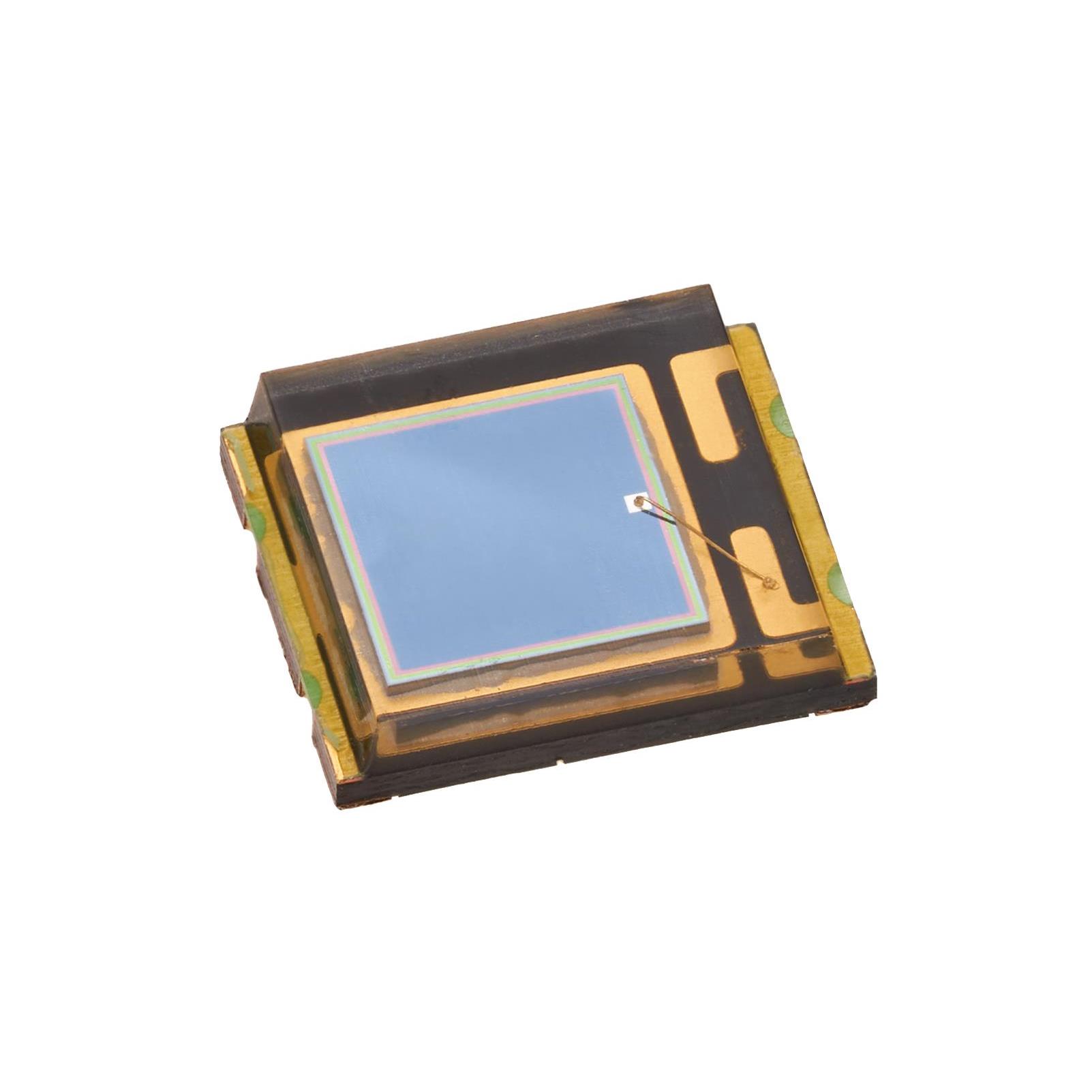
PDB-C171SM
SENSOR PHOTODIODE 660NM 2SMD
Luna Optoelectronics (Advanced Photonix)
Details
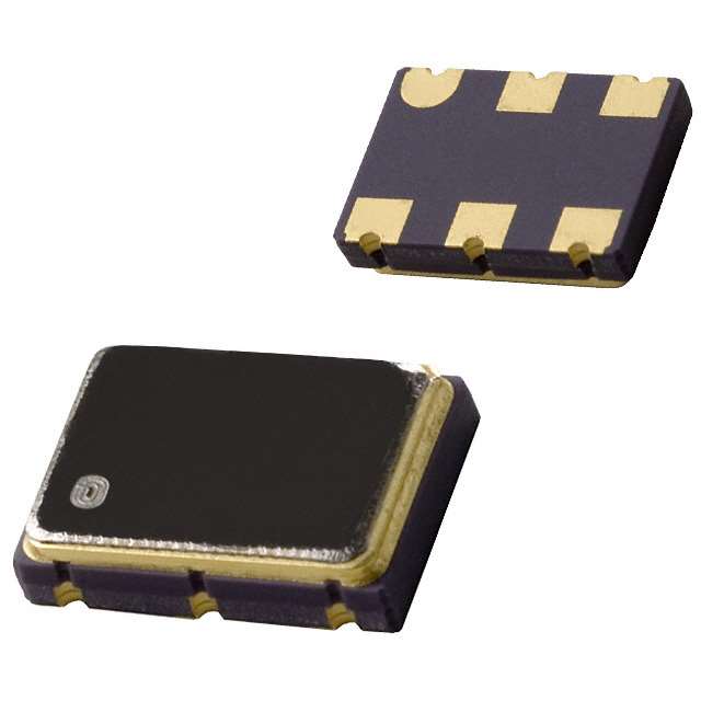
ECS-VXO-73-44.736-TR
XTAL OSC VCXO 44.7360MHZ CMOS
ECS Inc. International
Details
SK012DTP
SCR 1KV 12A TO252
Wickmann / Littelfuse
Details
VS-40HFL10S02
DIODE GEN PURP 100V 40A DO203AB
Vishay General Semiconductor – Diodes Division
Details
1SMB5928BT3G
ON SEMICONDUCTOR 1SMB5928BT3G Single diode Zener, general purpose, 13 V, 3 W, DO-214AA, 5 %, 2-pin, 150 °C
RHS10K
POT 10K OHM 25W WIREWOUND LINEAR
S87C51RA24
IC MCU 8BIT 8KB OTP 44QFP
Q8015N5TP
TRIAC 800V 15A TO263
ECS-VXO-73-35.328-TR
XTAL OSC VCXO 35.3280MHZ CMOS
M48T37V-10MH6F
IC RTC CLK/CALENDAR PAR 44SOH
STLC3055QTR
IC INTERFACE SPECIALIZED 44TQFP
VS-16FLR10S02
DIODE GP REV 100V 16A DO203AA
VS-85HFL100S05
DIODE GEN PURP 1KV 85A DO203AB
AD8612ARUZ
IC COMPARATOR 2 W/LATCH 14TSSOP
Q8010NH5TP
TRIAC ALTERNISTOR 800V 10A TO263
076-14-21-011
SENSOR PHOTODIODE 660NM TO46
VS-70HFLR40S02
DIODE GP REV 400V 70A DO203AB
QK008N5RP
TRIAC 1KV 8A TO263
AD834JNZ
IC MULTIPLIER QUADRANT 8DIP
PDB-C171SM
SENSOR PHOTODIODE 660NM 2SMD
TL16C550DRHB
IC ASYNC COMM ELEMENT 32-VQFN
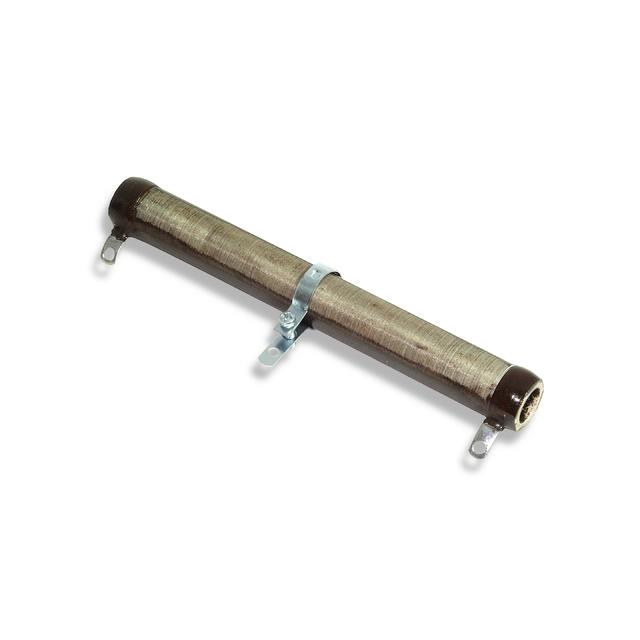
D50K5R0
ADJ PWR RES 5 OHM 50W CHAS MT
inter
agent
YAGEO
agent
EMIT
agent
TE Connectivity AMP Connectors
agent
Wickmann / Littelfuse
agent
3M
agent
Intersil (Renesas Electronics Corporation)
agent
B&K Precision
agent
Hirose Electric Co., Ltd.
agent
Zetex Semiconductors (Diodes Inc.)
agent
Keystone Electronics Corp.
agent
Omron Electronic Components
agent
application development in Hot Swap Controllers for ECS-F1HE335K: key technologies and success stories
2025-10-18
ECS-F1HE475K Digital Potentiometers highlighting the core functional technology articles and application development cases of Digital Potentiometers that are effective.
2025-10-17
application development in CODECS for ECS-F1CE225K: key technologies and success stories
2025-10-14
CFR-12JB-52-110R DC DC Switching Controllers highlighting the core functional technology articles and application development cases of DC DC Switching Controllers that are effective.
2025-10-13
1SMB5928BT3G
GCIXP1250BC
GW13J7K50E
MGA-87563-TR1
AD834JNZ
RJS225E
QK010N5TP
SWT-1.02-168
VS-16FLR10S02
D50K5R0
S87C51RA24
D25K100
STA015$013TR
VS-85HFL100S05
W6810ISG TR
AD8612ARUZ
OPB742
BTS7751GNUMA1
RHS10K
Q8006NH4TP
NJM2711F-TE1
D225K100
AD2S99APZ
BH2226FV-FE2
L6004V3TP
E2F-X2E1
RJS2K5E
PEF 20571 F V3.1
Q6010N5RP
RHS100E
QK016NH6RP
ISD17210SY
076-14-21-011
ST2042BD
EE-2002
Q4010NH5RP
ECS-VXO-73-35.328-TR
NJU7095D#
SN74ALVCH16374DL
QK006NH4TP
Q8016NH6RP
M74HCT374RM13TR
VS-40HFL40S02
application development in Hot Swap Controllers for ECS-F1HE335K: key technologies and success stories
On 2025-10-18 in
2
Application Development in Hot Swap Controllers for ECS-F1HE335K: Key Technologies and Success StoriesDeveloping applications for Hot Swap Controllers, such as the ECS-F1HE335K, involves leveraging several key technologies and methodologies to ensure reliability, efficiency, and performance. Here’s an overview of the key technologies and some success stories related to application development in this domain. Key Technologies1. Hot Swap Technology2. Field Programmable Gate Arrays (FPGAs)3. Microcontrollers and Embedded Systems4. Power Management ICs (PMICs)5. Communication Protocols6. Software Development Kits (SDKs)7. Real-Time Operating Systems (RTOS)1. Telecommunications Infrastructure2. Data Center Operations3. Industrial Automation4. Medical Devices5. Consumer Electronics Success Stories ConclusionThe application development for Hot Swap Controllers like the ECS-F1HE335K is driven by a combination of advanced technologies and innovative solutions across various industries. The success stories highlight the importance of reliability and uptime in critical applications, showcasing how hot swap technology can lead to significant operational improvements and customer satisfaction. As technology continues to evolve, the potential for new applications and enhancements in hot swap capabilities will likely expand, offering even more opportunities for innovation. The ongoing development in this field promises to enhance system resilience and operational efficiency across diverse sectors.
ECS-F1HE475K Digital Potentiometers highlighting the core functional technology articles and application development cases of Digital Potentiometers that are effective.
On 2025-10-17 in
2
ECS-F1HE475K Digital Potentiometers: Core Functional Technology and Application Development CasesDigital potentiometers, such as the ECS-F1HE475K, are pivotal components in contemporary electronic systems, offering precise control over resistance values across a multitude of applications. Below is an overview of the core functional technology and several application development cases that underscore their effectiveness. Core Functional Technology of Digital Potentiometers1. Digital Control: Digital potentiometers are manipulated through digital signals, commonly utilizing communication protocols like I2C, SPI, or UART. This digital control allows for accurate adjustments and seamless integration with microcontrollers and other digital systems, enhancing overall system performance. 2. Non-Volatile Memory: The ECS-F1HE475K features non-volatile memory, which ensures that the settings are preserved even when the device is powered down. This capability is essential for applications that require consistent performance without the need for recalibration after power loss. 3. Multi-Turn and Single-Turn Options: Digital potentiometers are available in both multi-turn and single-turn configurations. Multi-turn types offer finer resolution over a broader range, making them ideal for applications that require precise adjustments, while single-turn types are suited for applications needing quick and straightforward changes. 4. Resistance Range and Taper Options: These components come in various resistance values and taper options (linear or logarithmic), allowing designers to select the most appropriate type for their specific application requirements. 5. Integrated Features: Many digital potentiometers, including the ECS-F1HE475K, come with additional integrated features such as programmable gain amplifiers, temperature sensors, or analog-to-digital converters (ADCs), which enhance their functionality in complex electronic systems. Application Development Cases1. Audio Control Systems: Digital potentiometers are extensively used in audio equipment for functions like volume control, tone adjustment, and equalization. For example, in a digital mixing console, the ECS-F1HE475K can facilitate precise audio level adjustments, ensuring smooth transitions and maintaining high sound quality. 2. Industrial Automation: In industrial applications, digital potentiometers play a crucial role in motor control systems. By adjusting resistance in feedback loops, they help maintain precise control over motor speed and torque, thereby enhancing operational efficiency and performance. 3. Medical Devices: Digital potentiometers are integral to medical equipment for calibrating sensors and controlling critical parameters such as pressure, flow, and temperature. Their non-volatile memory ensures reliable operation over time, which is vital in healthcare settings where precision is paramount. 4. Consumer Electronics: In consumer devices like televisions and smart speakers, digital potentiometers are employed for user interface controls, including brightness, contrast, and volume adjustments. Their integration into touch-sensitive controls improves user experience by providing smooth and responsive adjustments. 5. Automotive Applications: Digital potentiometers are increasingly utilized in automotive systems for adjusting settings in infotainment systems, climate control, and electronic stability control. Their robustness and reliability make them well-suited for the demanding conditions of automotive environments. 6. Robotics and Automation: In robotics, digital potentiometers are used for sensor calibration and feedback control in servos and actuators. This capability allows for precise movement and positioning, which is essential for tasks that require high accuracy and reliability. ConclusionThe ECS-F1HE475K digital potentiometer exemplifies the versatility and effectiveness of digital potentiometers across various applications. Their ability to provide precise control, retain settings, and integrate seamlessly with digital systems makes them invaluable in modern electronic design. As technology continues to advance, the role of digital potentiometers is expected to expand, leading to even more innovative applications across diverse industries. Their adaptability and functionality will continue to drive advancements in electronic systems, making them a critical component in the future of technology.
application development in CODECS for ECS-F1CE225K: key technologies and success stories
On 2025-10-14 in
2
Application Development in CODECS for ECS-F1CE225K: Key Technologies and Success StoriesThe ECS-F1CE225K microcontroller from the ECS (Embedded Control Solutions) family is a versatile platform for embedded applications. Its capabilities, combined with CODECS technologies, enable developers to create innovative solutions across various domains. Below, we explore the key technologies that facilitate application development and highlight notable success stories. Key Technologies1. Real-Time Operating Systems (RTOS)2. Low-Power Design3. Communication Protocols4. Sensor Integration5. Data Compression and Encoding6. Machine Learning and AI7. Security Features1. Smart Home Devices2. Wearable Health Monitors3. Industrial Automation4. Smart Agriculture5. Telecommunication Devices Success Stories ConclusionThe ECS-F1CE225K microcontroller, in conjunction with CODECS technologies, has empowered developers to create a diverse array of innovative applications across multiple industries. By leveraging key technologies such as RTOS, low-power design, and advanced communication protocols, developers have successfully addressed the challenges of modern embedded systems. The success stories illustrate the microcontroller's versatility and effectiveness in real-world applications, paving the way for future advancements in embedded technology.
CFR-12JB-52-110R DC DC Switching Controllers highlighting the core functional technology articles and application development cases of DC DC Switching Controllers that are effective.
On 2025-10-13 in
5
Overview of CFR-12JB-52-110R DC-DC Switching ControllerThe CFR-12JB-52-110R is a specific model of a DC-DC switching controller that exemplifies the advancements in power management technology. It is designed to efficiently convert and regulate voltage levels in various applications, making it a critical component in modern electronic systems. Below, we delve deeper into the core functional technologies and application development cases that highlight the effectiveness of DC-DC switching controllers like the CFR-12JB-52-110R. Core Functional Technologies of DC-DC Switching Controllers1. Buck and Boost Conversion2. PWM Control3. Efficiency Optimization4. Feedback Mechanisms5. Protection Features6. Integrated Components7. Digital Control1. Telecommunications2. Consumer Electronics3. Industrial Automation4. Electric Vehicles (EVs)5. Renewable Energy Systems6. Medical Devices Application Development Cases ConclusionThe CFR-12JB-52-110R DC-DC switching controller represents a significant advancement in power management technology, offering high efficiency, flexibility, and reliability across a wide range of applications. Its integration into telecommunications, consumer electronics, industrial automation, electric vehicles, renewable energy systems, and medical devices underscores the versatility and critical role of DC-DC switching controllers in modern technology. As power demands continue to evolve, the importance of these controllers in providing efficient and reliable power management solutions will only increase, driving innovation and performance in various sectors.
Carol.inntraltd@gmail.com
Carol.Inntraltd
Carol.Inntraltd
Carol.inntraltd@gmail.com
lang_service_time
lang_select_kefu
Carol.inntraltd@gmail.com
lang_service_time
lang_select_kefu
Carol.inntraltd@gmail.com
0


")


")